Capabilities & Technologies
Our thick-film circuits or hybrid circuits are based on AL2O3 (aluminum oxide), AIN (aluminum nitride) and on stainless steel substrates.
The areas of application have expanded again and again due to the enormous reliability.
We have an extensive service portfolio for you with different process integration.
From the technology development of your thick-film hybrid circuit to the production of complex hybrid modules, assemblies and OEM products.
Download Prospekt "Dickschichtschaltungen und Hybridschaltungen"
|
Development
- Technology and development advice
- Editing the positions of conductor tracks and the layout
- Development of the circuit and programming of the algorithms of the processors and steering angles of commercial vehicles
- Development of the circuit and software for electronic detonators
for mining and tunneling
- Development of power electronics modules and heating controls
|
 |
|
Thick Film Technology
- resistance layers
- resistors
- We print capacitors and inductors on AL2O3, AIN and stainless steel substrates
- Standard sizes 4 "x6" // 101.6mm x 152.4mm
- Standard thicknesses AL2O3: 0.635mm and 1.0mm
- Other thicknesses: 0.25mm; 0.38 mm; 0.5mm, 0.76mm, 1.27mm
|
 |
|
Screen printing (info thick film technology)
- It is printed in the clean room, class 10,000
- Substrates made of AL2O3, AIN and stainless steel are printed
- Typical sizes 4 "x 6", special sizes on request
- Multilayer up to 9 resistance layers
- Two-sided printing
- Metallized vias (holes)
- Intersections and intersection points
- Conductor tracks and metallizations: Conductive pastes include Gold, Silver and Blndes with platinum and palladium.
Ag (silver 2 ... 3 mΩ), AgPd (silver palladium 15 ... 50 mΩ),
Pt (platinum 60 ... 100 mΩ), Au (gold 2 ... 7 mΩ),
PtPd (platinum palladium 30 ... 100 mΩ)
|
 |
|
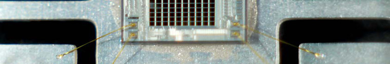
Wire Bonding
- Au Wire bonding (gold wire bonding)
- Al Wire Bonding (Aluminium wire bonding)
- We have different bonding systems with different bonding processes and use the necessary wire thickness for your hybrid circuit
|
 |
|
SMT (Sure Mount Technology) Technologie
- Clean room Class 100000 (Fed. Stand. 209d) Class 8 (ISO 14644-1)
- Discrete, active and passive components are mounted directly on the printed circuit board surface printed with solder past
- Circuit boards
- FR4 circuit boards
- Ceramic circuit boards made of aluminum oxide and aluminum nitride
- IMS (Insulated Metallic Substrate) printed circuit boards
|
 |
|
Assembly SMT (Sure Mount Technology) technology
- Fully automatic assembly line
- Vacuum oven to provide a void free soldering
- It is assembled in the clean room, class 100,000
- 0402 series resistors and capacitors, size 0201 if required
- Packaging DIL, SIL and other special components
- Epoxy coating
- We equip with fully automatic siplacers
- AOI and ICT
|
 |
|
Chip on Board Technologye (COB)
- A die (semiconductor without housing) is placed in solder paste or adhesive on a circuit board or substrates
- After soldering or curing the adhesive, Au (gold) or Au (aluminum) wires are bonded
- For protection, the die with bonding wires is cast and possibly the circuit board is cast with an epoxy resin for protection
|
 |
|
Resistance trim
- Our laser trimmer is also in the class 100,000 clean room
- Resistance values from 0.1 Ω to 5 GΩ
- TCR (Temperature Coefficient of Resistance) - 50ppm / ° C
* 1 ppm = 0.00001%
- Resistance trim on the top
|
 |
|
Function test and ICT (Inciruit Test)
- Is carried out in our class 100,000 clean room
- All printed circuit boards and thick-film circuits and hybrid circuits are 100% tested
- We also carry out special tests according to your specifications
|
 |
Quality
- ISO / TS 16949 certified
- Quality manual based on the Mil-STD-883 standard
- Standard procedure
- Special procedures according to customer requirements
- Lot tracing
- FMEA