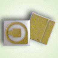
Ceramic Substrates
DCB substrates (Direct Copper Bond) or DBC substrates (Direct Bond Copper) or CPC substrates (Copper Plated Ceramic), thin-film circuits, thick film circuits and PCTF (Plated Copper on Thick Film) substrates are in the power electronics, LED technology (LED submount) and laser diode technology (laser diode submount) due to the small size, mechanical strength and good thermal conductivity, used more frequently.
In automotive electronics, especially for hybrid cars, wind power technology, DC converters, HF radio technology ceramic substrates are used increasingly. The requirements for high performance electronic are growing.
We supply ceramic substrates for ceramic circuit boards, thick-film circuits, DCB substrates (Direct Copper Bond), DBC substrates (Direct Bond Copper) and thick film hybrids, Rogers PCB and composite substrates in the lot size ONE, small and medium quantities.
An outstanding heat transfer can reached if you solder or glue your circuits on our MMC, (Metal Matrix Composit) like metal-diamond composites. With this high performance material for electroncs cooling you can get much higher performance.
We can provide substrates with 4different metallization technologies PCTF (Plated Copper on Thick Film), DCB substrates, Thick-Film-substrates, Thin-Film-substrates and Ag-ENIG Substrates. The finish metalisation is up to your application and the follow-up process.
Finish of NiAu (Nickel / Gold) for soldering, glue and Al-Wire bonding (Aluminium-Wire), Finish of NiPdAu (Nickel / Paldium / Gold) for soldering, glue and Al-Wire and Au-Wire bonding. We can process an Ag (Silver) finish also.
Overview Metallization
Any power application can achive even better heat dissipation with void free solder connections. Test our Vacuum Soldering-System and reach a much higher performance of your power applications.
|
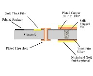
Core Technology: Plated Copper on Thick films (PCTF ®) Technology
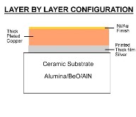
- PCTF is a patented manufacturing process to produce layers of plated copper (up to .010" thick) 25µm- 150µm, allowing high current capacity in excess of 50 Amps as well as excellent heat spreading and low thermal resistance. Solid metal vias ensures significant improvement in thermal management and electrical performance.
- This cost effective technology is extremely versatile. In addition to its basic copper plated metalization, we offer a complete range of thick film resistors and thick film gold. PCTF® technology allows you to complement your high power plated copper tracks with thick film multilayer circuitry, thus combining power and logic on the same substrate (SMART POWER).
- Tin, Nickel, and Gold (electrolytic & electroless) finishes over bare copper allow for excellent soldering, wire bonding (aluminum and gold) and eutectic die attach. New is the electro plating of AuSn (Gold / Tin) bumps or on laser submounts.
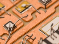
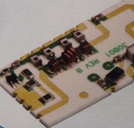
- The PCTF® substrate provides an ideal solution for both the assembly of surface mount components and chip-on-board technology.
- We services a broad range of industries from telecommunications and computers to power supplies, electro-optical, laser and medical electronics, covering military, industrial and commercial range applications.
- Typical applications include RF power amplifiers and LNA’s, optical switches, LED, filters, high-density DC/DC converters, driver circuits, thermoelectric coolers, power hybrids, power modules, smart power, power packages, chip carriers and other power assemblies.
|


|
DCB (Direct Copper Bond) oder DBC (Direct Bond Copper) Substrates on Alumina (AL2O3) and Aluminium Nitride( AIN). DBC is widely acceptable and a timeproven technology for power electronic products due to its high thermal conductivity, hight current capacity and heat dissipation of the high-purity copper on ceramic.
- By varying copper and ceramic thickness and ceramic type one can affect a resulting in CTE (coefficient of thermal expansion) value of the total system an avoid a CTE mismatch with different semiconductor devices.
- NiAu (Nickel / Gold) or NiPdAu (Nickel / Paladium / Gold) plating finish enable a broad range of economical assembly techniques: SMT soldering, low and high temperature die attach, Al (Aluminium) and Au (Gold) wire and ribbon bonding.
Ag finish is possible also.
- Our LVM (low volume manufacturing) DBC / DCB programm will be available for orderes that may not meet the minimum requirements for a normal production run with other manufactures.
|

|
LOW COST AgENIG THICK FILM SUBSTRATES are a cost effective, reliable, RoHS compliant ceramic substrates with AgENIG metallization without costly platinum/palladium materials.
- These versatile, high performance metallized ceramic substrates are an economic substitute for currently used expensive thick film materials containing platinum/palladium and are RoHS compliant.
- New AgEnig lower cost metallized ceramic substrates combine silver thick film processing with (ENIG) electroless nickel and immersion gold plating.
- They are 30% lower in price than commonly used Pd-Pt-Ag (platinum / palladium / Silver) substrates.
- AgENIG ceramicsubstrates offer a number of significant performance advantages. First, solder leaching, Typical of conventional thick film substrates, is greatly reduced. This is especially important when using lead free soldering at temperatures of 260°C or higher. The track´s resistivity is improved tenfold to 1 mΩ/square and the substrates can be used up to 170°C continuous operation temperature.
|
 |
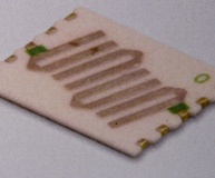
Thick film substartes with burned Ag (silver) and Au (Gold) paste in single and multilayer technology ia a alternative solution for your printed circuit board (PCB).
- Hybrids are made on ceramic PCB´s usual. With our innovation we now make them on stainless steel and titanium. These ceramics PCB´s, stainless steel PCB´s and titanium PCB´s enable products to work well in hostile environment and have greater reliability over time than PCB´s.
- Applications for hybrid circuits are endless and include temperature sensors, pressure sensores, flow sensors and stain gauges, water pump applications, baggage x-ray machines, scientific instruments, data loggers, components for cars, solar cells and electrical safety devices jsut to name few.
|
 |
Thin film substrates metallized with Titanium and Thungsten
- Our PCTF Technology use thick film substrates and thin film substrates depending from the application and the required line / space.
- In addition to ceramic submounts the Gold Tin option can also be applied to Copper Tungston submounts and laser bars.
- Laser submounts and LED submounts on AIN with a thin film seed layer help to produce submounts with a outstanding performance.
|
 |
|
